


Jensen Huang’s GTC Blockbuster Product Faces Setback. Nvidia Kyber NVL144 Delayed to 2028, Is PCB the Key Bottleneck?



AI Podcast


Nvidia’s Kyber NVL144 AI architecture faces a 12-month delay, now expected in 2028, due to manufacturing bottlenecks in its 78-layer orthogonal backplane. Technical complexities, including ultra-high-density PCB requirements and signal integrity, have hampered mass production. Failed attempts at transitional "back-to-back" designs and the cancellation of the 4-compute-chip Rubin Ultra version further constrain projected performance. These infrastructure challenges, coupled with uncertainties surrounding CPO technology integration for larger NVL576 systems, create potential market share opportunities for competitors like AMD and Google, who may capitalize on Nvidia’s slowed development pace in high-end AI training hardware.
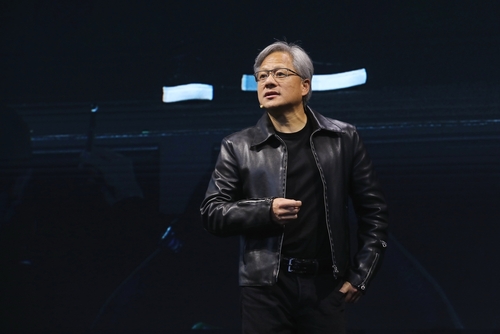
TradingKey - On the morning of July 6, semiconductor industry research firm SemiAnalysis posted six consecutive tweets on platform X, disclosing that Nvidia's ( NVDA) rack-scale AI architecture, Kyber NVL144, has encountered a major delay.
This blockbuster product, which was high-profiled by Jensen Huang at the GTC conference just three months ago, is now reported to be delayed by more than 12 months, with its release pushed back to 2028.
The Core Challenge: Manufacturing Difficulties of 78-Layer PCB Middle Boards
SemiAnalysis pointed out that the direct reason for the delay of Kyber NVL144 lies in the manufacturing process bottleneck of the PCB midplane. This key component, which NVIDIA calls the "orthogonal backplane," is the core to achieving efficient interconnection of 144 GPUs within a single rack.
Unlike the horizontal layout adopted by traditional servers, the Kyber architecture utilizes a vertical stacking design. Through this midplane, it achieves a 90-degree vertical interconnection between the compute trays and the switch trays, completely eliminating signal attenuation and space occupancy issues caused by traditional cables.
However, this seemingly ordinary circuit board represents the extreme limit of current PCB manufacturing processes. According to technical analysis, the midplane uses a hybrid material of M9-grade copper clad laminate + quartz cloth + PTFE, with up to 78 layers (produced by pressing three 26-layer boards together), and a line width/spacing of ≤25μm, to meet the ultra-high-speed signal integrity requirements under a 448G+ SerDes rate.
While this design can theoretically achieve higher computing density, it faces a series of challenges in actual manufacturing, such as yield control, impedance consistency, and thermal design.
Industry insiders stated that there are currently very few manufacturers worldwide capable of mass-producing this ultra-high-density PCB, and the manufacturing cost is extremely high.
As alternative solutions suffer successive setbacks, scale expansion has stalled.
Faced with Kyber's manufacturing difficulties, Nvidia had attempted to develop a transitional solution—the NVL72x2 back-to-back rack architecture. This solution placed two Oberon racks back-to-back, expanding the scale domain via pure copper NVLinks in an attempt to bypass the manufacturing bottlenecks of the Kyber midplane.
However, this plan was ultimately canceled due to strong opposition from cloud service providers (CSPs) and hyperscalers. They believed that such a design was not only structurally complex but also carried extremely high operational and maintenance costs, making it difficult to deploy in large-scale data center environments.
To make matters worse, the 4-compute-chip version of the Rubin Ultra originally planned by Nvidia was also canceled, leaving only the smaller 2-compute-chip version, whose actual performance is roughly half that of the former.
This means that even if the Kyber racks are ultimately delivered on schedule, the computing power ceiling per rack has already been significantly lowered.
Larger-scale systems face uncertainty, presenting opportunities for competitors
In addition to the Kyber NVL144, uncertainty also looms over Nvidia's larger-scale NVL576 system. This solution integrates eight rack-level units into a higher-compute cluster using CPO (Co-Packaged Optics) technology. However, SemiAnalysis pointed out that given the current challenges facing CPO technology, the NVL576 may also be delayed or limited to small-batch shipments.
CPO technology is regarded as key to next-generation data center interconnects, but its mass production readiness remains to be verified. Nvidia plans to apply it to its next-generation Feynman platform.
This series of delays and cancellations has given competitors AMD and Google an opportunity to catch up. SemiAnalysis noted that Nvidia currently lacks a proven solution to scale out the scale-up domain of Rubin Ultra, which leaves room for products like AMD's MI500X or Google's TPUv8i Broadfly to surpass Rubin Ultra in scale-up capabilities.
As Nvidia slows its pace in advancing rack-level AI infrastructure, competitors are poised to capture more share in the high-end AI training market.
This content was translated using AI and reviewed for clarity. It is for informational purposes only.
Recommended Articles









Comments (0)
Click the $ button, enter the symbol, and select to link a stock, ETF, or other ticker.