

Intel Joins Musk’s Terafab Project, Can the World’s Largest Chip Factory Really Be Built?

Intel is joining Elon Musk's Terafab project, a mega-scale chip manufacturing initiative with SpaceX, Tesla, and xAI. This collaboration aims to accelerate Terafab's goal of an annual 1 terawatt of computing power, supporting AI and robotics development. Terafab, with an estimated $20 billion to $25 billion investment, will utilize a vertically integrated model. Intel's expertise in chip design, manufacturing, and packaging is expected to validate the project's feasibility and provide Intel with a crucial anchor client for its foundry strategy. The project's massive scale could significantly impact the global semiconductor landscape.
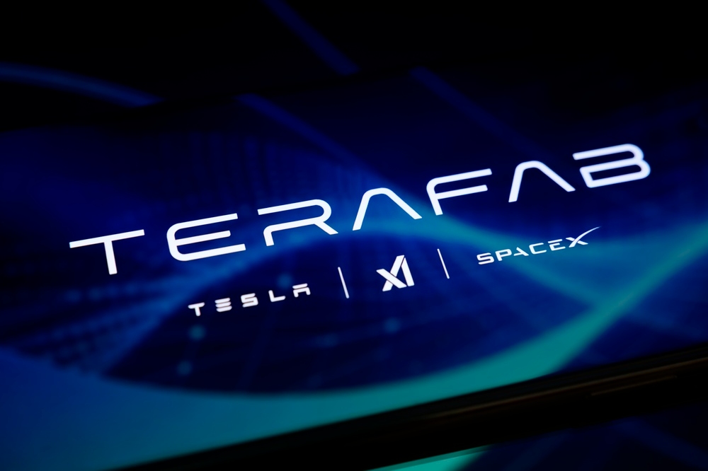
TradingKey - On April 7 local time, Intel ( INTC) officially announced via Elon Musk's social media platform X that it is joining the Terafab mega-scale chip manufacturing project jointly advanced by SpaceX, Tesla ( TSLA) and xAI, with both parties set to engage in deep collaboration in semiconductor manufacturing and high-performance chip R&D.
Intel stated in its statement that its technical expertise at scale in the fields of ultra-high-performance chip design, manufacturing, and packaging will accelerate Terafab's goal of achieving an annual computing capacity target of 1 terawatt, providing core support for the future development of artificial intelligence and robotics.
This partnership also marks Intel officially becoming a key partner in Musk's Terafab project, joining SpaceX, Tesla, and xAI in advancing this ambitious chip manufacturing initiative.
What is a Terafab?
Elon Musk officially launched the Terafab chip manufacturing project on March 30, driven jointly by Tesla, SpaceX, and xAI. The first phase will be established at the north side of the Giga Texas campus in Austin, Texas, with a planned total investment of $20 billion to $25 billion. The project aims to produce chips with an annual computing power of over 1 terawatt, a scale equivalent to approximately 2% of the total current global chip factory capacity and 50 times the world's current annual AI computing output (about 20 gigawatts).
According to the plan, 80% of the chips produced by Terafab will be deployed in space for SpaceX’s interstellar AI satellite data centers and radiation-hardened chip needs, while 20% will be allocated for terrestrial applications, including Tesla FSD, Cybercab robotaxis, and Optimus humanoid robots. Musk specifically highlighted that the project will manufacture dedicated chips for Tesla’s humanoid robots.
Unlike TSMC’s "pure-play foundry" industry standard—where the company only converts client designs into physical wafers without involvement in design—Terafab will utilize a disruptive vertical integration model. It will complete chip design, lithography, manufacturing, memory production, advanced packaging, and testing within a single facility, creating a complete closed loop from raw materials to finished products. This model allows for rapid iteration cycles, reduces transport between different nodes, and significantly improves the speed of chip updates.
Regarding scale, Terafab’s initial target is 100,000 wafers per month, with a final goal of scaling to 1 million—equivalent to roughly 70% of TSMC’s total current global production capacity.
According to the roadmap, annual chip output is expected to reach 100 billion to 200 billion units. The facility will be constructed in two phases: Phase I is projected to start production in the second half of 2027 with mass production in 2028, and Phase II is slated for full completion by 2030.
Terafab will mainly produce two categories of chips: one optimized for edge inference for Tesla FSD, Cybercab, and Optimus humanoid robots, and another specializing in high-performance radiation-hardened chips for space-based AI systems.
Why Intel’s inclusion is significant?
Prior to Intel's official announcement of its participation, Elon Musk's Terafab mega-scale chip manufacturing project had been a "controversial topic" of intense debate within the semiconductor industry.
Many industry insiders believe that since Tesla and SpaceX have no prior experience in chip manufacturing, the semiconductor industry's high technical barriers and complex process requirements call Terafab's feasibility into question, leaving its prospects widely doubted.
However, Intel's entry is likely to break this impasse. Analysts suggest that Intel can provide not only its advanced 18A process node and EMIB packaging technology but also leverage its global fab operational expertise to help Terafab quickly scale to mass production.
As a global semiconductor leader, Intel is the first chip giant to publicly announce its involvement in the Terafab project, providing a clearer roadmap for a project that previously seemed far-fetched.
Intel stated in a declaration: "Our capability to design, manufacture, and package ultra-high-performance chips at scale will help accelerate Terafab’s mission to produce 1 terawatt (TW) of computing capacity annually, driving the future of AI and robotics."
Industry analysts estimate that the total investment for the Terafab project could reach $20 billion to $25 billion. If the project progresses as planned, its annual capacity of 1 terawatt would be 50 times the current global output of AI chips, potentially reshaping the global semiconductor landscape.
Currently, the two parties have not disclosed specific details of the collaboration. Core issues, such as the scale of investment, capacity allocation, and intellectual property ownership, remain to be revealed.
What are the implications for Intel’s foundry strategy?
This collaboration not only opens a significant window for Intel's long-sought foundry business but also marks a critical step in the chip giant's transformation journey.
Intel CEO Lip-Bu Tan stated in a subsequent declaration: "Elon Musk has an outstanding track record in reshaping industry landscapes, which is exactly what the transformation and upgrading of today's semiconductor manufacturing sector urgently require. Terafab represents a major paradigm shift in the future of silicon logic, memory, and packaging manufacturing. Intel is honored to be a partner and to work closely with Musk to advance this highly strategic project."
For Intel, which is currently in a critical period of transformation, this collaboration serves as a much-needed timely boost.
In recent years, Intel has been actively promoting its IDM 2.0 strategy, attempting to attract external customers through its "Intel Foundry" business. However, even after achieving mass production for its 18A process node, the foundry division has consistently lacked an anchor customer like Tesla to justify its capital expenditures.
Meanwhile, Musk's enterprises span several high-compute demand fields such as electric vehicles, aerospace, and artificial intelligence, with a massive, long-term, and certain demand for custom chips—Tesla's Optimus humanoid robot is expected to reach an annual production of 1 billion to 10 billion units, SpaceX plans to launch 1 million AI data center satellites, and xAI requires massive computing power to support large model training. These demands will provide Intel with a stable source of orders.
Prior to this, Intel had been continuously seeking external foundry customers but failed to announce any substantial agreements. The Terafab project, however, directly targets the 2nm advanced process. If Intel can successfully complete this mission, it will not only prove to the market that its manufacturing capability is sufficient to meet the chip demands of top-tier tech companies, but also potentially restore its reputation, which has lagged behind TSMC and Samsung in the field of advanced process nodes.
This content was translated using AI and reviewed for clarity. It is for informational purposes only.
Recommended Articles


Comments (0)
Click the $ button, enter the symbol, and select to link a stock, ETF, or other ticker.