


Samsung Works With Nvidia to Develop 8-Layer HBM4E, Targeting a 20% Speed Boost Over Initial Samples



AI Podcast


Samsung Electronics is developing an 8-layer HBM4E for Nvidia, targeting 17 to 18 Gbps/pin to address supply shortages, helping Samsung's stock rebound 1.17% on August 31, Asia-Pacific time. Nvidia's newly released NVHBM solution integrates the memory controller into the HBM base die, boosting bandwidth and reducing power consumption. While Samsung's in-house DRAM and foundry capabilities position it as a key competitor in the custom HBM market, development collaboration does not guarantee a mass production contract, and volume details remain undisclosed.

TradingKey - On August 31, Asia-Pacific time, according to South Korea's Seoul Economic Daily, Samsung Electronics is developing 8-layer HBM4E per the requirements of Nvidia (NVDA), targeting speeds of 17 to 18 Gbps/pin, an approximately 20% increase from the 14.4 Gbps speed of Samsung's initial HBM4E samples. The product will be used for NVHBM. As of press time, Samsung officials have not commented on the report.
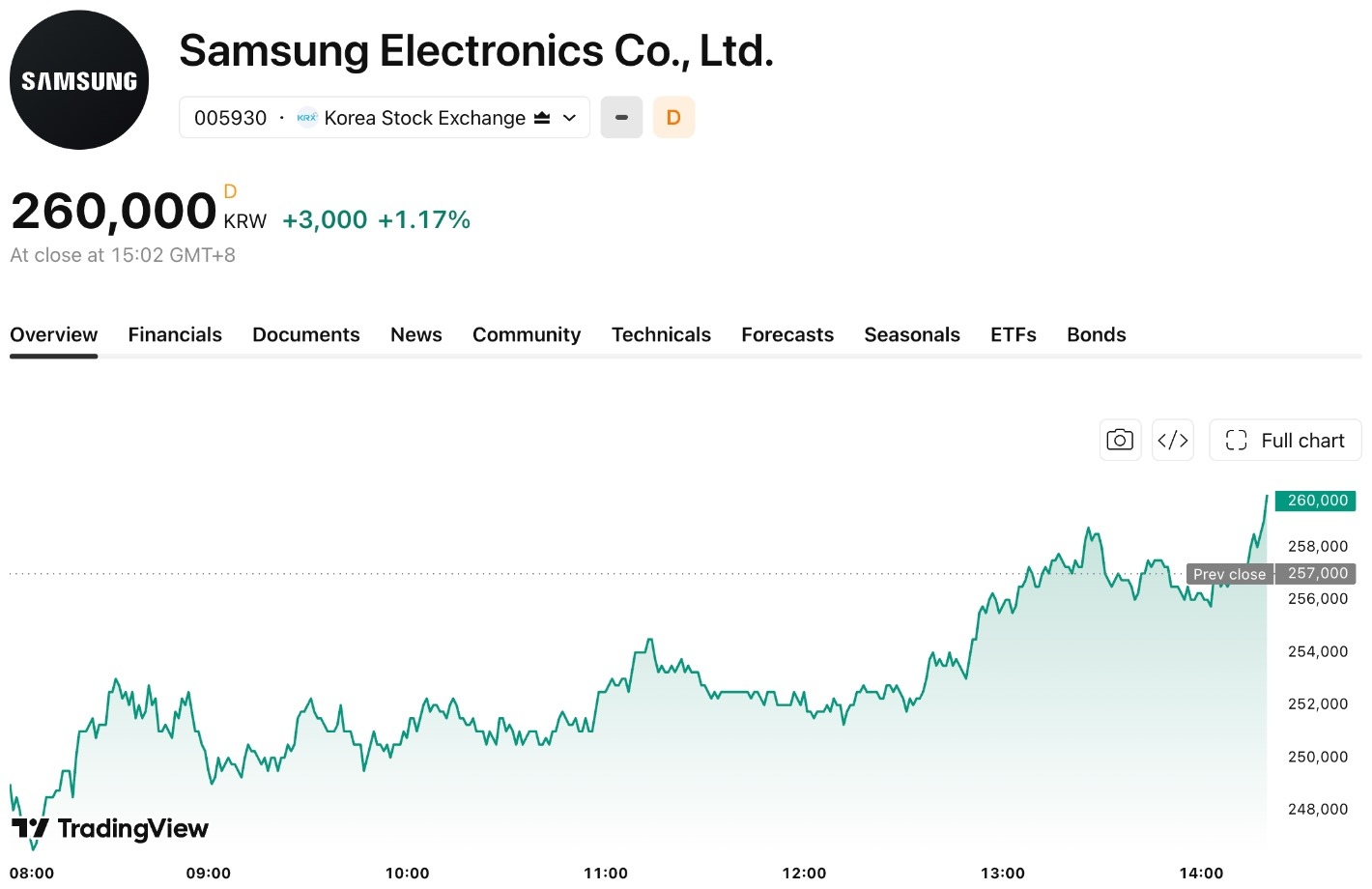
Boosted by news of the HBM4E development, Samsung Electronics reversed earlier losses to rise in afternoon trading. During the morning session, hit by factors including Federal Reserve rate hike signals, US chip tariff risks, and new South Korean policies raising margin requirements on leveraged products, South Korean stock markets opened generally lower, with Samsung Electronics tumbling over 4% at one point to 246,000 won (about $179).
After the news broke in the afternoon, the stock rebounded into positive territory, closing up slightly by 1.17% at 260,000 won.
[Source: TradingView]
Nvidia requested that Samsung adopt an 8-layer HBM solution this time, abandoning its previously planned 12-layer and 16-layer configurations. The reduction in layers lowers the difficulty of back-end processes such as wafer thinning and stacking packaging, which helps improve yields and expand production capacity. Market consensus views this as Nvidia's strategy to address HBM supply shortages.
On August 26, Nvidia officially released NVHBM, an HBM solution designed for custom AI chip customers using the NVLink Fusion platform.
This solution moves the memory controller from the main chip to the base die of the HBM stack. Compared with the standard HBM4E solution, bandwidth is increased by up to 30%, power consumption is reduced by 15%, and the available compute area on the main chip is increased by up to 25%. Annapurna Labs, a subsidiary of Amazon (AMZN), is its first partner.
Customized products such as NVHBM require design and manufacturing capabilities for both DRAM chips and logic base dies. As Samsung operates both DRAM manufacturing and foundry businesses, it can produce HBM DRAM wafers and logic base dies in-house, making it widely regarded in the industry as a key supplier competing in the custom HBM market.
However, cooperation during the development phase is distinct from securing volume production orders. Samsung's collaboration with Nvidia to develop 8-layer HBM4E does not imply that it has secured a mass supply contract for NVHBM. In currently available public information, specific supply volumes and timelines between the two parties have not been disclosed.
This content was translated using AI and reviewed for clarity. It is for informational purposes only.
Recommended Articles








Comments (0)
Click the $ button, enter the symbol, and select to link a stock, ETF, or other ticker.