

AI Memory Chip Demand Surges, SK Hynix and Samsung Race to Significantly Expand Capacity


AI Podcast
Driven by surging AI demand, SK Hynix plans to triple wafer capacity by 2034, targeting 1 million monthly DRAM units by 2030, with significant expansion at Yongin and Cheongju. Samsung Electronics is considering its first new packaging facility in 35 years in Gwangju and investing in a Vietnam testing site. Both companies are aggressively expanding advanced packaging and HBM capacity, recognizing them as critical to the AI chip supply chain and competitive advantage.
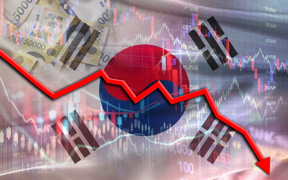
Tradingkey - As the deployment of AI technology accelerates, global demand for high-performance memory chips continues to surge. South Korea's two leading semiconductor giants, SK Hynix and Samsung Electronics, have recently announced major capacity expansion plans to strategically position themselves across the AI chip supply chain.
SK Hynix: Wafer Capacity to Triple by 2034
SK Group Chairman Chey Tae-won recently revealed to Nikkei Asia that SK Hynix plans to triple its total wafer capacity by 2034 to meet the growing demand for memory chips driven by artificial intelligence; he expects wafer capacity to double within five years.
SK Hynix has shared its expansion plans with major suppliers, with a core goal of increasing monthly DRAM wafer capacity from the current approximately 550,000 units to about 1 million units by around 2030, with approximately 200,000 units coming from its Wuxi factory in China.
Most of the additional capacity will come from the Yongin semiconductor industry cluster. SK Hynix has significantly advanced the construction schedule for the Yongin wafer fab, with the first phase expected to be completed early next year. The first phase of the Yongin plant is divided into six cleanrooms; each cleanroom will gradually add 60,000 units of monthly capacity upon activation, enabling the first plant alone to add 360,000 units of monthly DRAM capacity by the first half of 2030.
Meanwhile, SK Hynix's M15X wafer fab in Cheongju is scheduled to begin operations in the second half of this year, with an initial monthly capacity of 40,000 units, which is expected to increase to approximately 80,000 units by 2027. Combined with the expansion contributions from Yongin Phase I and M15X, SK Hynix's monthly DRAM wafer capacity is poised to reach approximately 1 million units between 2030 and 2031.
Following its domestic expansion, SK Group also plans to collaborate with Nvidia ( NVDA) to build an AI data center in Japan between 2028 and 2029.
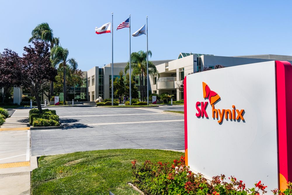
Samsung Electronics: First New Packaging Facility in 35 Years
Samsung Electronics is considering the construction of a new advanced semiconductor packaging plant in Gwangju, South Korea. This would mark Samsung's first new packaging base in 35 years and its first major semiconductor production facility launch in 11 years since the groundbreaking of the Pyeongtaek campus.
According to South Korean media reports, Samsung may formally announce this investment plan as early as the meeting between the South Korean President and heads of major conglomerates on June 29. Once the Gwangju plant is completed, Samsung's packaging business footprint will extend southward from traditional strongholds in Chungcheong Province (such as Onyang in Asan and Cheonan) to the Honam region.
Regarding its technical roadmap, Samsung is aggressively expanding HBM back-end processing capacity at its Cheonan site, aiming to increase monthly capacity for thermal compression bonding (TCB) to 231,000 units and hybrid copper bonding (HCB) to 19,500 units by the end of 2026. Furthermore, Samsung plans to fully transition its HBM stacking process from TCB to HCB in 2029, highlighting its sustained commitment to next-generation advanced packaging technologies.
In terms of overseas operations, Samsung intends to invest approximately $1.5 billion in Vietnam to build a semiconductor testing facility. Construction on the facility began in April 2026, with formal production expected to commence in November 2027.
Analysts point out that as demand for AI computing power continues to explode, advanced packaging and high-performance memory chips have become strategic high ground in semiconductor industry competition. SK Hynix and Samsung are leveraging massive capital expansion and clear capacity planning to actively seize market opportunities in the AI era.
This content was translated using AI and reviewed for clarity. It is for informational purposes only.
Recommended Articles


Comments (0)
Click the $ button, enter the symbol, and select to link a stock, ETF, or other ticker.