


SK Hynix and SanDisk Debut New HBF Storage Standard as Google Joins Ecosystem



AI Podcast


On August 3 ET, the HBF Alliance, led by SK Hynix and SanDisk, released the first High Bandwidth Flash (HBF) standard under the OCP framework. Positioned between HBM and SSD, HBF utilizes 3D NAND stacking to bridge the gap between high bandwidth and capacity required for AI inference. With Google and Tenstorrent involved, the open standard leverages the UCIe interface for broad processor compatibility. Additionally, SK Hynix unveiled its 10th-generation 375-layer 4D NAND, signaling a push toward large-scale implementation. The commercial success of HBF now hinges on industry adoption rates within hyperscale data centers.
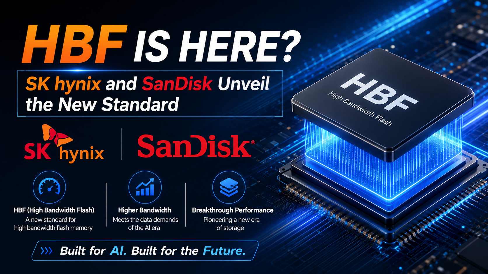
TradingKey - On August 3 ET, the opening day of the Flash Memory Summit 2026 in California, US, SK Hynix ( SKHY) and SanDisk ( SNDK) jointly released the first standard specification for High Bandwidth Flash (HBF).
The two companies reached an intent of cooperation in August last year and officially established the HBF Alliance under the OCP framework in February this year. It took only half a year from the official launch of the alliance to the release of the standard specification.
Among the members of the HBF Alliance, besides SK Hynix and SanDisk, there is also Google ( GOOGL) and AI chip startup Tenstorrent. Google's entry means that from the very beginning, HBF has targeted the actual needs of hyperscale data centers, rather than remaining in the laboratory concept stage.
HBF is positioned neither as a replacement for HBM nor as an upgraded version of SSD, but rather to carve out a new storage tier between the two.
As the AI industry shifts from model training to inference applications, a contradiction is becoming increasingly sharp: while HBM has high bandwidth, its capacity is limited and costly, making it difficult to support the parameter scale of large models; SSD has abundant capacity, but its read and write speeds face hardware bottlenecks, failing to match the real-time requirements of AI inference.
HBF combines NAND flash with mature 3D stacking technology from the HBM process, aiming to provide both high bandwidth and large capacity, adding a specialized storage option for AI inference servers.
The standard specification defines two capacity configurations, based on 8-layer and 16-layer NAND chip stacking respectively, supporting up to 512GB. Bandwidth is divided into three grades (Grade 1~3), covering approximately 0.4TB/s to 3.0TB/s.
HBF adopts the industry-standard UCIe interconnect interface, which can flexibly adapt to processors of different architectures, such as GPUs and CPUs. The specification was released by OCP, the world's largest open data center technology collaboration organization, as a general open standard for the industry rather than a proprietary corporate solution.
In addition, during the summit, SK Hynix publicly showcased its 10th-generation (V10) 375-layer 4D NAND flash wafers and products for the first time, with energy efficiency increased by 2.5 times compared to the previous generation, and mass production expected early next year. The company also stated that it will take this opportunity to promote the large-scale implementation of HBF in the AI storage market.
For the memory chip industry, Google's entry has injected key momentum into the building of the HBF ecosystem. Whether HBF can truly fill the gap in the memory tier depends on the adoption speed and scale of end customers. However, the finalization of the standard specification at least provides a clear starting point for this goal.
This content was translated using AI and reviewed for clarity. It is for informational purposes only.
Recommended Articles











Comments (0)
Click the $ button, enter the symbol, and select to link a stock, ETF, or other ticker.