


Gemini Architecture Written Directly Into Silicon: Technical Details of Google’s New AI Inference Chip “Frozen v2” Revealed, Processing per Unit of Power Consumption Increased by up to 10 Times



AI Podcast


Google is developing the "Frozen v2" server chip, designed to hardcode Gemini model architecture directly into hardware to address severe AI compute shortages. By embedding model logic into silicon, the chip aims to improve inference efficiency by 6 to 10 times in energy consumption. This vertical integration strategy mirrors Apple’s approach, aiming to lower AI costs and optimize performance. However, this deep software-hardware coupling poses significant risks; should Gemini’s architecture undergo major shifts, the chips risk obsolescence. Currently, the project serves as a technical test platform, with potential deployment targeted for 2028.

TradingKey - According to The Information, citing two people familiar with the matter, Google ( GOOGL) is developing a brand-new server chip that can directly hardcode the underlying architecture of its Gemini large model into the chip's hardware, thereby significantly improving the operational efficiency of delivering AI services to users.
This AI inference chip, internally codenamed "Frozen v2", directly addresses Google's current pain point of a severe shortage of AI computing power. Sources revealed that the computing power gap has triggered internal resource conflicts, even forcing Google Cloud to turn down many external customer orders. The R&D team estimates that once the chip is officially deployed, the number of tokens processed per unit of power consumption will reach 6 to 10 times that of the latest generation of Google's existing self-developed AI chips.
[Source: TradingView]
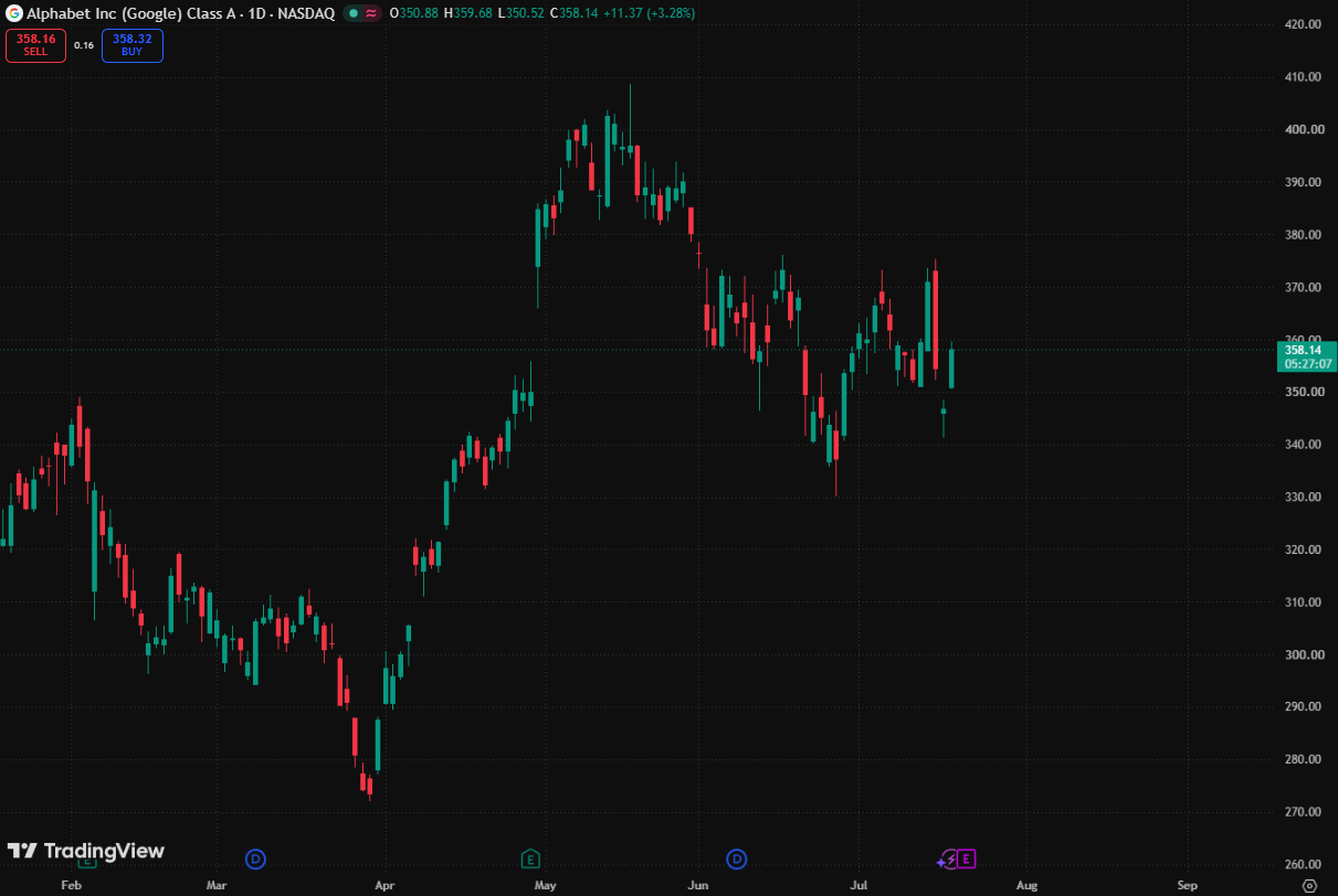
Stimulated by the news, Google's stock price performed strongly today, hitting an intraday high of $359.67. As of press time, it was still up 3.28% at $358.14, with the stock price returning above its 5-day, 10-day, and 20-day moving averages.
Why Is It Called Frozen?
The origin of the codename "Frozen" stems from its core design concept: permanently etching part of the Gemini large model's computing logic onto the silicon hardware—akin to "freezing" the software in the chip. Engineers are still finalizing the chip's core functional modules and the collaborative solutions for various components, and Google plans to deploy this AI chip as early as 2028.
The Frozen project aims to carve out a brand-new AI chip product line to complement Google's existing Tensor Processing Units (TPUs), rather than replace them.
Currently, the most widely used AI chips—Nvidia ( NVDA) GPUs and Google TPUs—are all general-purpose chips that can adapt to multiple different large models. However, when general-purpose chips run any model, they need to execute a large number of time-consuming logic judgments in real time; in contrast, the Frozen v2 AI inference chip directly builds in the underlying computing logic adapted to the Gemini series models, significantly reducing chip computing steps and data movement, thereby achieving a qualitative leap in inference efficiency.
People familiar with the matter said that this dedicated AI chip can respond to user queries faster, which is expected to support Google in launching entirely new AI application scenarios.
Google’s Strategic Bet on Frozen v2 Chip: Deep Integration of Hardware and Software
The technical roadmap of Frozen v2 means Google is making a strategic bet—wagering that it will continue to use the underlying architecture of the current Gemini large model. Only if subsequent iterations of the Gemini model adopt an underlying architecture consistent with the one used when the AI chip was designed can they run properly on the chip.
People familiar with the matter added that Google can still perform iterative optimization on the chip, including updating the built-in model weights—weights are the core parameter configurations that determine how the AI model answers questions.
A Google spokesperson responded that the company's teams "continuously research, develop, and test various innovative technologies, striving to achieve ultimate performance and energy efficiency for users and enterprise customers," adding that "not all R&D projects will eventually go into mass production, but this comprehensive technical exploration is a core part of our full-stack proprietary technology roadmap."
Google’s Software-Hardware Integration Ambition for Frozen v2 Chip
The revelation of the Frozen v2 AI chip reflects Google's deep strategic logic in the AI infrastructure sector, with AI compute anxiety being the primary driver. As the size of Gemini models continues to swell, the energy efficiency ceiling of general-purpose chips is drawing closer. Embedding large model logic directly into hardware represents a radical solution to break through the energy efficiency bottleneck of AI compute.
This also signals that Google is replicating an "Apple-style" vertically integrated path of combining software and hardware. From its self-developed TPUs to the Frozen series of dedicated AI chips, Google is attempting to establish a full-stack closed loop from model architecture to chip design in the AI era. If this path proves successful, it will drastically drive down AI inference costs, paving the way for Gemini's commercialization.
However, the risks are equally impossible to ignore. The deep coupling of chips and models means that once Gemini's underlying architecture undergoes a major iteration, Frozen AI chips could quickly become obsolete. Google's positioning of Frozen v2 as a "technical test platform" rather than a mass-production product precisely demonstrates that this path still requires time to be validated.
This content was translated using AI and reviewed for clarity. It is for informational purposes only.
Recommended Articles







Comments (0)
Click the $ button, enter the symbol, and select to link a stock, ETF, or other ticker.