

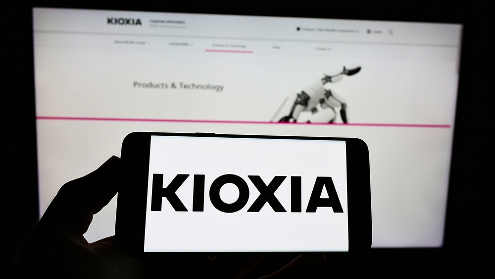
Memory Giant Kioxia Ships 332-Layer Flash to AI Data Centers, Shares Surge Over 10% After Wild Swings


AI Podcast
Kioxia has commenced sampling its 10th-generation 332-layer BiCS FLASH 3D memory, targeting AI data center demand. The chip features a 59% increase in bit density and significant improvements in energy efficiency and interface speeds. Despite initial volatility during Asian trading on July 3, the stock rebounded by 10.07% to 83,940 yen as markets recognized the technological advancement. Positioned to compete with Samsung and SK Hynix in the high-stack memory sector, Kioxia leverages proprietary CBA technology. Mass production is scheduled for 2027 at the Kitakami plant, reinforcing its strategic focus on the global AI infrastructure supply chain.
TradingKey - During the Asian trading session on July 3, global memory chip giant Kioxia announced that it has officially begun sampling its 10th-generation BiCS FLASH 3D flash memory technology products to customers. Boasting a 332-layer stacked architecture, this 1Tb TLC chip is directly aimed at the explosive demand for high-capacity, low-power storage in AI data centers, signaling a new phase in the "memory war" surrounding AI infrastructure.
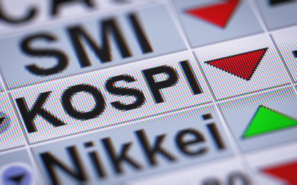
Although the Nikkei 225 Index was under pressure in early trading and Kioxia's stock price initially fell by over 9% due to market sentiment fluctuations, the stock quickly turned positive and surged over 10% as technical details of the new product were digested, staging a powerful rebound. As of press time, Kioxia's stock price was up 10.07% to 83,940 yen. Previously, benefiting from the AI boom, Kioxia's market capitalization had surpassed Toyota's to rank first in Japan.
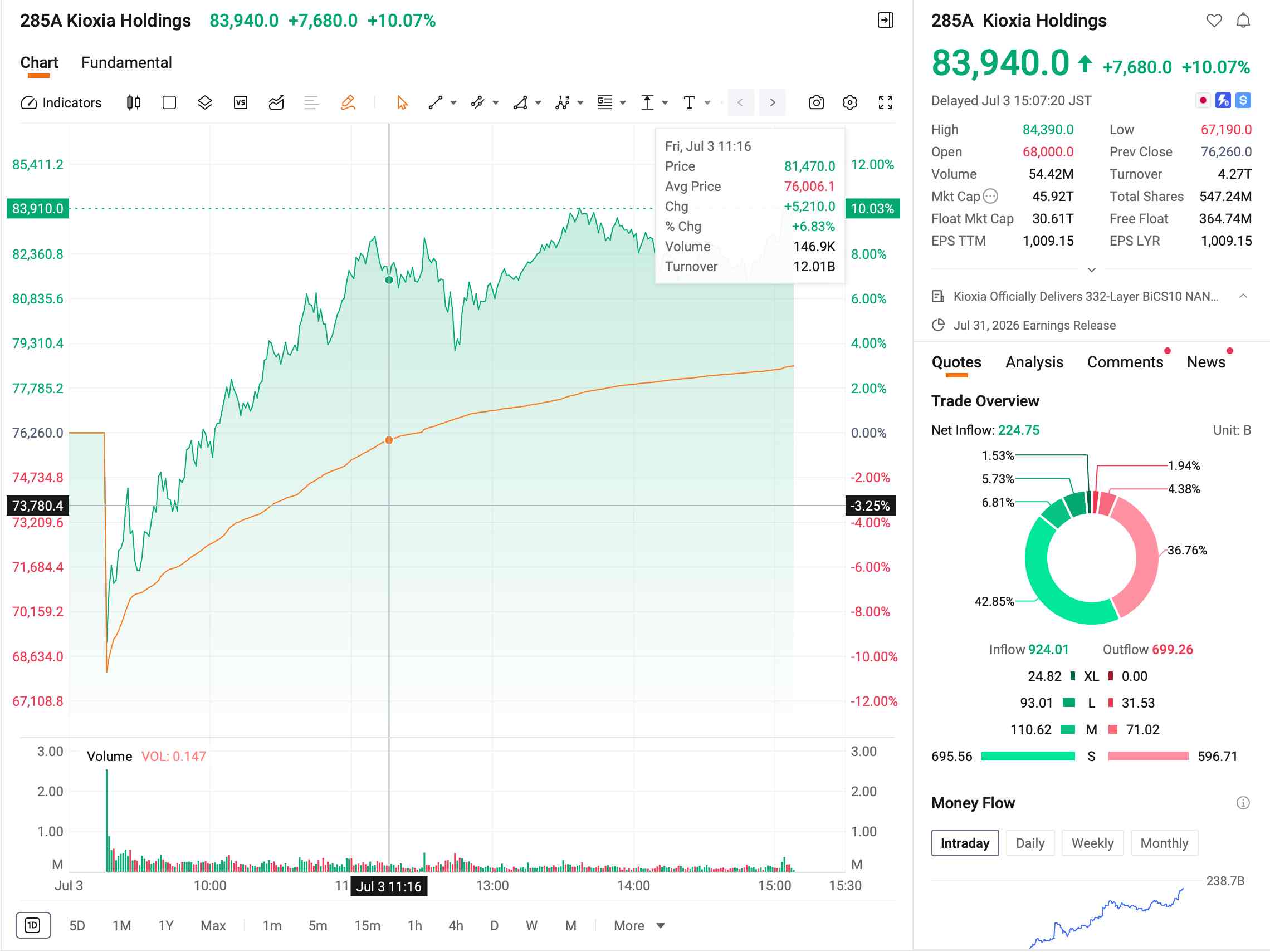
[Source: Futu]
It is reported that this 10th-generation product, which is currently sampling, represents a major technological leap. Relying on the "CMOS directly Bonded to Array" (CBA) technology introduced in the eighth generation, the next-generation flash memory achieves a NAND interface speed of 4.8Gb/s, a 33% increase over the previous generation. Meanwhile, the vertical stacking of up to 332 layers combined with optimized lateral density has resulted in a staggering 59% increase in bit density. More importantly, its read and write energy efficiencies have improved by 18% and 30% respectively, directly addressing the pain point of high power consumption in data centers.
The new product is manufactured at Kioxia's Fab2 in Kitakami, Iwate Prefecture, Japan, which is its only facility globally capable of scaling up the production of 332-layer flash memory.
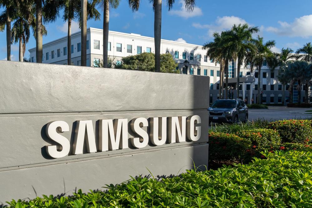
In the face of fierce competition from rivals like Samsung and SK Hynix in the 300+ layer flash memory space, Kioxia is going all out to secure its position in the AI data center supply chain by leveraging the first-mover advantage of BiCS 10. According to market sources, mass production of the product is expected to commence at the Kitakami plant in 2027.
This content was translated using AI and reviewed for clarity. It is for informational purposes only.
Recommended Articles


Comments (0)
Click the $ button, enter the symbol, and select to link a stock, ETF, or other ticker.